A Guide to Buying Gold Finger PCBs

Gold Finger PCBs from Gold Finger PCB Manufacturer, also known as gold-plated edge connectors, feature gold-plated contacts along their edges, facilitating reliable electrical connections between PCBs and external components. These specialized PCBs are commonly used in devices that require frequent plugging and unplugging, such as memory cards, computer motherboards, and expansion boards. The gold plating on the edge connectors provides several advantages, including excellent conductivity, corrosion resistance, and protection against wear and tear.
Factors to Consider When Buying Gold Finger PCBs:
- Connector Design and Quality: The design and quality of the gold-plated connectors are crucial considerations. Ensure that the connector design aligns with your specific application requirements and that it offers a secure and durable connection. High-quality gold plating should provide sufficient thickness and uniformity, ensuring long-term performance and reliability.
- Gold Plating Thickness: The thickness of the gold plating on the edge connectors significantly impacts the PCB's performance. Generally, thicker gold plating provides better conductivity and increased resistance to corrosion. It is advisable to select Gold Finger PCBs with a minimum gold plating thickness of 30 micro inches (0.762 microns) to ensure optimal performance and durability.
- Compatibility and Specifications: Before purchasing Gold Finger PCBs from Gold Finger PCB Manufacturer, carefully review the compatibility requirements and specifications of your intended application. Consider factors such as board dimensions, pin arrangement, and voltage/current ratings to ensure a perfect fit and seamless integration with your electronic device.
- Manufacturing Standards and Certifications: Opt for Gold Finger PCBs that adhere to recognized manufacturing standards and certifications. Look for certifications like ISO 9001 and UL (Underwriters Laboratories) to ensure that the PCBs meet stringent quality control measures and safety standards.
- Supplier Reputation and Support: Choosing a reliable and reputable PCB supplier is crucial to guarantee the quality and consistency of the Gold Finger PCBs. Research customer reviews, request samples, and evaluate the supplier's technical support and customer service capabilities to make an informed decision.
Conclusion:
When it comes to ensuring seamless connectivity and reliable electrical connections, investing in high-quality Gold Finger PCBs is a wise choice. By understanding the key factors discussed in this comprehensive guide, you'll be equipped with the knowledge to make an informed decision while purchasing Gold Finger PCBs from Gold Finger PCB Manufacturer. Remember to consider connector design
Exploring the Benefits of Multilayer PCBs
Among the different types of PCBs available, multilayer PCBs have gained significant popularity due to their ability to accommodate complex electronic designs and provide numerous benefits. In this article, we will delve into the advantages of multilayer PCB and understand why they have become an integral part of the electronics industry.
Increased Design Flexibility
Multilayer PCBs offer unparalleled design flexibility, allowing engineers to create intricate and compact electronic designs. With multiple layers of copper traces and insulating material sandwiched together, these PCBs provide ample space for routing signals and power planes. The additional layers enable the designer to optimize the placement of components, reduce signal interference, and enhance the overall performance of the circuit.

High Density and Miniaturization
As electronic devices continue to shrink in size, the demand for miniaturized PCBs has grown exponentially. Multilayer PCBs are an ideal solution to meet these requirements. By utilizing multiple layers, they can achieve higher-density interconnections without compromising on performance. The ability to stack multiple layers of copper traces vertically allows for the efficient use of space, making multilayer PCBs suitable for compact devices such as smartphones, wearables, and medical implants.
Enhanced Signal Integrity and EMI Shielding
Multilayer PCB exhibit superior signal integrity characteristics compared to their single or double-layer counterparts. The multiple internal power and ground planes help reduce noise and provide better signal quality. By separating sensitive analog or high-speed digital signals from noise-inducing components, these PCBs minimize cross-talk and electromagnetic interference (EMI), ensuring reliable and high-quality performance.
Enhanced Reliability and Durability
Reliability is of utmost importance in electronic devices, especially those used in mission-critical applications. Multilayer PCBs demonstrate superior reliability due to their enhanced structural integrity. The multiple layers act as reinforcements, providing increased rigidity and resistance to external stresses, such as vibrations and mechanical impacts. Additionally, the use of high-quality materials and advanced manufacturing techniques ensures the durability of these PCBs, making them suitable for applications that require prolonged operation in harsh environments.
Streamlined Manufacturing and Cost Efficiency
Although multilayer PCB may appear more complex than their single or double-layer counterparts, advancements in manufacturing technology have made them more accessible and cost-effective. With the availability of automated manufacturing processes and optimized fabrication techniques, the production of multilayer PCBs has become more streamlined. Furthermore, the reduced size and increased functionality of multilayer PCBs often result in fewer overall components, simplified assembly processes, and reduced production costs.
To Know more Common Flexible Printed Circuit Design Errors
The bundling engineer and electronic creator are offered a decent open door by flexible PCB. You can shape, curve, turn, and overlay these flexible electronic wiring frameworks into interminable layered setups.
The following is given a few well-known ways how Flexi punch can make a plan more powerful, producible, and prepared for creation.
Dividing between weld cushions and nearby follows: You can uncover the edges of the contiguous guide follows when the openings of cover film or patch veil are made bigger. This can bring about causing shorts however just when weld spans between connector pins or cushions. To oblige the cover film or bind veil situation resistance there is a necessity for additional space between a patch cushion and a nearby conductive follow.

Emphasize focuses in guides: In the two fields that are in introducing and dynamic flexing applications, there is the utilization of Flex hardware yet an unbending PCB might make issues in a flex circuits board follow designs. At the foundation of weld cushions, the guide follows with sharp corners and intense crossroads become normal emphasize focuses yet the condition is that the region close to them ought to be flexed. For guide, turn focuses a decent adaptable circuit design will have a smooth range.
Bind veil or cover film openings: Adaptable hardware can show layered change during the manufacture interaction yet solely after openness to processes like pumice cleaning, copper plating, or potentially carving. The plans of adaptable hardware configuration rules need bigger resistances to oblige resulting enrollments for cover film, stiffeners, or pass-on cutting.
Welded joints excessively near bowing point: With the assistance of an intermetallic obligation of the patch compound to the copper follow, a binding joint is framed. Nonetheless, the hints of the copper are regularly adaptable however the districts that have been fastened become extremely unbending and resolute.

The primary concern is that with standard PCB programming, the planning of a flex circuit can bring about some serious manufacturability and unwavering quality issues. It is dependably something great to work with your adaptable circuit provider or an adaptable circuit plan master as they flex the plan before starting manufacture or it can make the design straightforwardly from a netlist. This will ensure that to address your issues the Adaptable PCB configuration can be produced.
Process of First Article Inspection in PCB Assembly
The initial item inspection process is a very important step in the creation of your PCBA China. Following the submission of your design and the assembly process required to produce units that meet your defined specifications by your PCBA assembler, the first boards are often considered to be the "first item" manufactured.
Prototypes and PCBA pre-production samples are not the first articles since they often use a distinct manufacturing method or piece of machinery. Furthermore, first article PCBAs do not always depart a PCB manufacturing line as the first products. Inspection at this step shows if production engineers or technicians have comprehended and taken into account your needs in their typical manufacturing procedures.
The initial article inspection procedure fulfills two crucial goals. The first is to check and confirm that all requirements listed in the documentation are satisfied. Establishing the manufacturing Plan of Record (POR) for continuing production is the second step. The POR must be duplicated continuously after it is set up to guarantee that all future production complies with specified specifications.
The first article construction procedure is crucial not just for fresh or initial designs but also each time a modification to the design is made.
Inspection of a first article PCBA assembly China should be a meticulous procedure that involves verifying that every single need that has been listed satisfies the specification. This has to be verified concerning:
Dimensions, voltages, resistance, and any other attributes that may be measured have to be recorded and contrasted with the requirements for the comprehensive design.
Manufacturing Issues: Any challenges, issues, or worries encountered during the PCBA process should be reviewed for modifications and fixes.
Source validation entails confirming that each component and material utilized in the PCBA adheres to its manufacturer's standards.
These procedures will identify any potential problems during the first article construction before moving forward with PCBA China manufacturing. Any problems then have time to be corrected before full production begins.
Modifications may be required to the solder process profiles, assembly process flow, tools, consumables, and build or test documentation. The customer may need to think about asking for a design revision if a product design defect is at the base of the problem to address it and take the necessary corrective action.
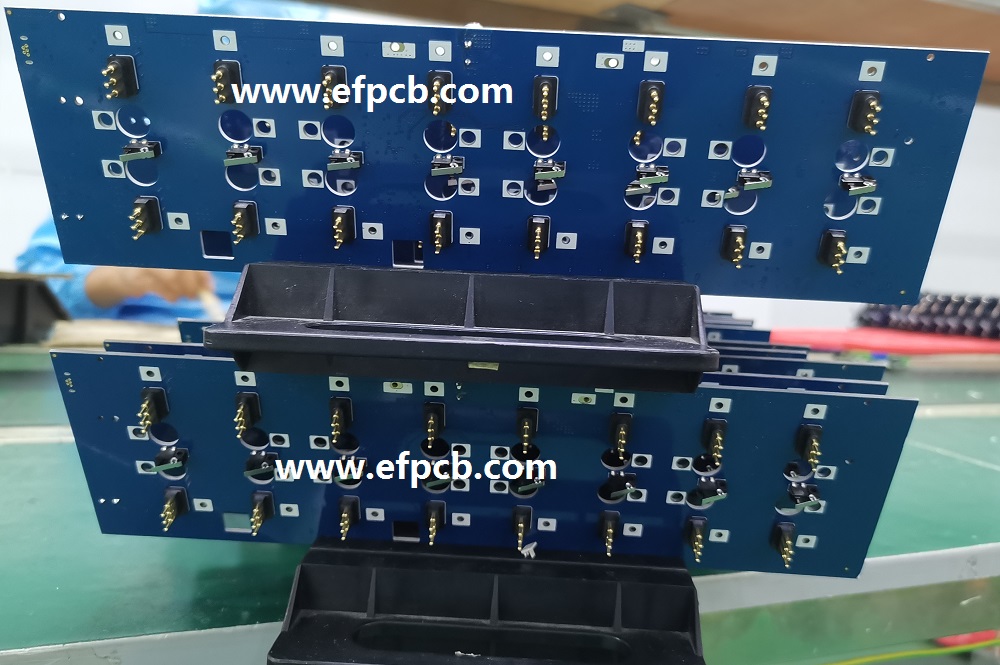
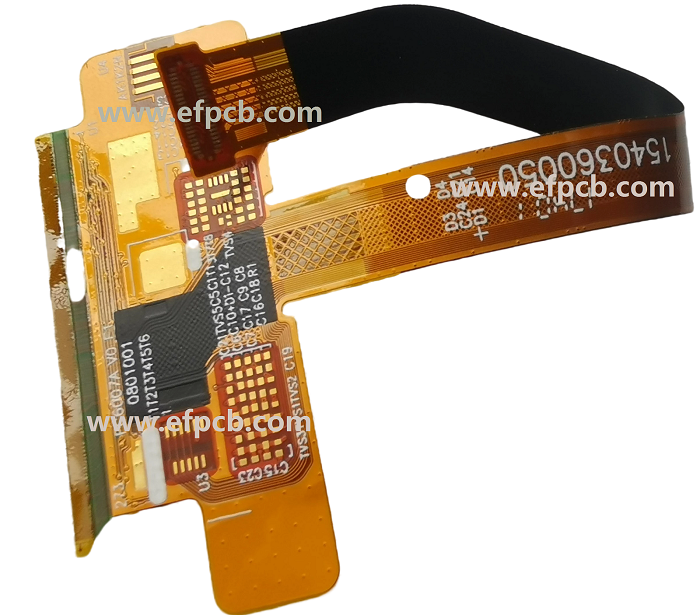
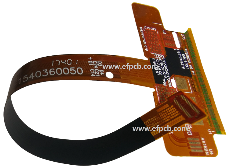
Flexible Printed circuit board assembly
Flexible circuits are members of the electronic and interconnection families. These are made with a skinny insulating polymer film that has a conductive circuit pattern affixed thereto. These are typically furnished with a skinny polymer coating to shield the conductor circuits. The characteristic of the flexible board is that the computer circuit board with an understandable pattern and also the arrangement of the components, and it's highlighted by the malleable base material. Flexible PCB manufacturer with flexible materials that have high stretching capacity, like plastics. The pliability comes in handy when the PCB has to shift or move without damaging the board components and connections. There are many sorts of flexible PCBs available within the market. Each can perform different electronics and intercommunication works. The foremost common variations of flex PCBs are - Single-sided PCB circuits, Double-sided PCB circuits, Multi-layer PCB circuits, Rigid-flex circuit, and Sculptured PCB flex circuits.
The benefits of those flexible circuits include- space-saving because it requires only 10 percent of the first conventional PCB thereby helping in packaging and installation. These flexible ones have lesser solder joints thereby reducing loopholes and improving the reliability of assorted parts. They work with every market available component and may work under extreme conditions of temperature wear and tear with better cooling and versatile installation.
Flexible circuits have a range of applications in numerous fields. The flexible circuits are developed to produce reliability, cost-saving, and long-lasting performances within the installed components. These are used maximum in antennas, laptops, LCD televisions, cell phones, and whatnot! These communication devices have seen leaps in development with the emergence of flex PCBs. However, the uses of the flex circuits don't seem to be limited here only. it's also employed in hearing aids, satellites, printers, and calculators the ultimate product after using flexible PCB is reduced volume and weight as compared to the traditional PCBs. It also meets all its requirements of high density, reliability, and minimizing space requirements. Flexible PCBs are relatively expensive, not cost-effective, and are slightly insufficient within the carrying capacity of the components. Hence combining rigid and versatile circuits is a perfect solution for manufacturing purposes. Rigid boards are generally attached with flexible circuits in a way that their advantages will be utilized in different PCB designs.
Know about the Schematic of Printed-Circuit-Board

Despite high-speed circuitry's critical nature in the design process, often, one of the last steps is Printed Circuits layout. To high-speed PCB layout, there are many aspects; volumes have been considered. A high-speed layout is addressed from a practical perspective. Helping newcomers gain a sense of the different considerations they must consider while designing layout boards for high-speed circuitry is the main aim. But to benefit those who have been away from board layout for a while, it is also intended as a refresher. Minimizing time-consuming, reducing design time, and improving circuit performance is crucial.
The rigid type is the most used and common type of Printed Circuit Boards, but another type that you may think of using is the flex one after getting yourself familiar with it. It is now more available as more manufacturers are providing this kind.
The Schematic
A good layout starts with a good schematic although there is no guarantee. When drawing a schematic, you must be generous and thoughtful and think about signal flow through the circuit. A good flow on the Circuits Board as well is present in a schematic having a steady and natural flow from left to right. On the schematic, put as much useful information as possible. The engineers, technicians, and designers working on this job will be most appreciative. As the designer is no longer there, customers ask to help with a circuit sometimes. For high-frequency signal transmission and impedance control, this makes the board a perfect match.

Used as the base in most electronics, Printed circuit boards (PCBs) are the boards. They are used both as the wiring area for the socketed and surface-mounted components and as a physical support piece. Out of another composite material, composite epoxy, or fiberglass, PCBs are made most commonly. Most PCBs are composed of only a single layer and for simple electronics are simple. Multiple layers up to twelve can be present in more sophisticated hardware such as motherboards or computer graphics cards.
In many other electronic devices, such as Cell phones, Radios, TVs, and Digital cameras, Printed Circuits can be found although they are most often associated with computers.
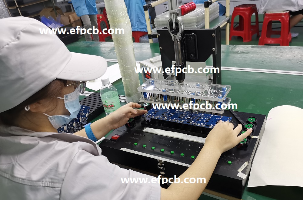
PCB Assembly Process Gets Benefitted From the SMT Assembly

SMT PCB assembly China has grown in importance as a result of the quick growth of information and communication technologies. The main task is to physically insert passive components like resistors, capacitors, and diodes while melting tiny quantities of hot solder paste onto circuit boards. Let's examine SMT assembly technology in more detail.
The technique of soldering electronic components to a printed circuit board (PCB) is known as SMT assembly technology. Small quantities of molten solder paste are utilized in this procedure to join the component leads to pads on the PCB surface. Automated machinery is frequently used in SMT assembly to place and install the components on the PCB.
The advantages of the PCB assembly process it brings
It simplifies assembly
There is no requirement for lead shaping because the component leads are surface attached to the pads. Compared to through-hole technology, where the component leads must be shaped before being placed into holes drilled in the PCB solder connections, this makes SMT PCBA assembly China considerably easier and quicker.
It is reliable
Because they are less susceptible to vibration and stress, surface mount components are often more dependable than their through-hole counterparts. Additionally, the likelihood of component failure at cold-solder junctions is significantly decreased when solder paste is used rather than liquid solder.
Experience using fine-pitch components
Excellent pitch components may be used in SMT assemblies, which is not achievable with through-hole technology. In situations where space is at a premium and component density is high, this can be a significant advantage.
Their variability
SMT assembly technique is very adaptable and may be utilized for a variety of applications, including telecommunications, medical devices, industrial control systems, and consumer electronics.
The capacity of PCBs to use mixed technology
Through-hole and surface-mounted component PCBs are also conceivable using SMT assembly technology. When creating an audio mixing board with both fixed controls (through-holes) and sliding faders or potentiometers, for example, this is helpful since space restrictions require the usage of both types of connections (SMD).
SMT Assembly Technology Uses
The following are some applications using SMT PCB assembly China technology:
- electronic devices
- Telecommunications
- medical equipment
- systems for industrial control
- defense and aerospace systems


